本次会议旨在推动集成电路技术的持续发展,并促进学术界、产业界和研究机构的紧密结合。预计将有来自宾夕法尼亚大学、复旦大学等世界各地学术界和产业界的500多位著名专家学者及优秀研究生代表参加,共同探讨集成电路技术的最新发展和应用前景。
大会设有技术研讨会以及海报展示和社交活动,内容覆盖AI电路至3D集成技术,旨在促进业界的学术交流。此外,大会还将颁发优秀学生和青年学者论文奖,以鼓励创新研究。
ICSICT是中国举办的规模最大、影响最广的固态器件和集成电路技术国际会议之一,每两年举办一次。自1986年起,ICSICT已成为VLSI电路设计者、系统集成商、IC制造商、器件工程师以及CAD/CAE工具开发者展示最新进展、发展和研究成果的重要平台。大会不仅促进了学术界与工业界的交流,更为参与者提供了一个共享信息和兴趣的绝佳机会。
本次会议的具体进程:

主题讲座信息:
1. Dr. Paul Penzes, Vice President, Qualcomm, USA
K1-1: 9:00-09:45, Oct. 23, 2024, Wednesday
Title: Low-Power On-Device Computation for Future AI Expansion
Abstract:
Artificial intelligence (AI) has emerged as the primary driver of future semiconductor revenue growth with a projected ~$1 trillion market by 2030. The AI silicon market is dividing into a cloud-based high-performance market and a cost and power constrained edge market as vendors balance performance requirements, energy consumption, bandwidth, and privacy concerns. This presentation highlights the importance of low-power on-device ML computation in system-on-chip (SoC) processors at the edge and discusses methods to optimize power and performance considering manufacturing variation, dynamic workloads, and aging effects, including adaptive methods to respond to on die voltage variation and strategies to improve robustness and yield by design and EDA.
Biography:
Dr. Paul Penzes currently serves as Vice President of Engineering at Qualcomm, overseeing the Design Technology and Computer-Aided Design teams. Qualcomm stands at the forefront of the fabless industry, pioneering cutting-edge semiconductor technologies and advanced circuit techniques for high-volume chip manufacturing. Under Paul's leadership, his team spearheads research and development in low-power, high-speed circuits using cutting-edge process technologies, emphasizing scalability and robustness through advanced design automation. Prior to his role at Qualcomm, Paul contributed to the development of advanced design methodologies and circuit techniques at Broadcom (now Avago) as part of the Office of the CTO's team. Broadcom, renowned as a leading semiconductor design house, provided a fertile ground for Paul's diverse R&D expertise. Earlier, Paul served as chip lead at Myricom, a startup affiliated with Caltech, where he specialized in developing low-latency, high-speed interconnect chips. With over 20 years of experience in the semiconductor industry, Paul has made significant contributions to both research and development, resulting in numerous publications and patents. Paul holds a BS, MS, and PhD from the California Institute of Technology.
2. Prof. Myung Hoon Sunwoo, Ajou University, Korea
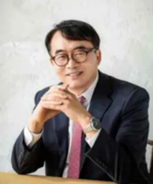
K1-2: 9:45-10:30, Oct. 24, 2024, Thursday
Title: How can AI and DL help Digital Healthcare?
Abstract:
The advent of Deep Learning/Artificial Intelligence (DL/AI) technology has opened a new era in disease diagnosis by developing many practical applications in the interdisciplinary convergence of ICT and medical applications. Medical big data enables the application of newly developed ICT technologies to increasingly popular medical fields. This presentation introduces the recent progress in AI and DL-based medical diagnosis and applications. In addition, the Medical Image-Based Intelligent Diagnosis Solution (MIIDS) Research Center integrates new interdisciplinary technologies through joint research with universities, hospitals, and companies. The MIIDS Center has developed various disease diagnosis networks, including jaundice, Alzheimer's, cardiac arrhythmia, mechanical ventilation weaning prediction, etc.
Biography:
Prof. Myung Hoon Sunwoo received B.S., M.S., and Ph.D. degrees from Sogang University in 1980, KAIST in 1982, and the University of Texas at Austin in 1990, respectively. He worked for ETRI in Korea (1982-1985) and Motorola DSP perations in Austin, Texas (1990-1992). Since 1992, he has been with Ajou University in Suwon, Korea, where he is currently a professor. He has authored numerous papers, holds over 120 patents, and has received over 60 awards. He has been an Associate Editor of IEEE TVLSI (2002-2003) and a coeditor of several books, including “Selected Topics in Biomedical Circuits and Systems,” with Prof. Minkyu Je at KAIST in 2021. He served as the General Chair of ISCAS 2012 in Seoul and General Co- chair of ISCAS 2021 in Daegu, Korea. He has been an IEEE CASS Distinguished Lecturer (2009–2010) and has served on the IEEE CASS BoG (2011–2016) and the VP-Conferences (2018–2021). During his term as CASS VP-Conferences, he founded the IEEE International Conference on Artificial Intelligence Circuits and Systems (AICAS) in 2019. AICAS has become the CASS Premier Conference in 2021. He is the director of the Medical Image-Based Intelligent Diagnostic Solutions (MIIDS) Research Center. His research interests include AI/DL circuits and systems and medical imaging diagnosis. He is the IEEE CASS President (2024–2025) and is an IEEE Fellow.
3. Prof. Zhong Lin Wang, Georgia Institute of Technology, USA
K2-1: 10:45-11:30, Oct. 23, 2024, Wednesday
Title: Piezotronics of the third- and fourth-generation semiconductors
Abstract:
The classification of semiconductors is best given based on their crystallographic structures, which are the “DNA”s of general materials. The first generation semiconductors (Si, Ge) and the second generation semiconductors (GaAs) have a common characteristic that their crystal structures are cubic, so they exhibit the highest crystallographic symmetry. For the third generation semiconductors, such as GaN. SiC and ZnO, they have the hexagonal crystal structure. As for the fourth generation semiconductor such as Ga2O3, it has a monoclinic structure. Therefore, the non-centrosymmetric crystal structures at lower-symmetry for the third- and fourth-generation semiconductors make them distinctive different from the Si and GaAs owing to the piezoelectric effect that is generated by the polarization of ions in the crystal. A piezoelectric potential (piezopotential) is generated in the crystal by an externally applied strain. Electronics fabricated by using the inner-crystal piezopotential as a “gate” voltage to tune/control the charge transport behavior is named piezotronics, with applications in strain/force/pressure triggered/controlled electronic devices, sensors and logic units. Using the piezoelectric polarization charges at the pn junction to control charge carrier separation or combination process in optoelectronics is called the piezo-phototronic effect. This talk will focus on how to use piezo-phototronic effect to tune the efficiency of LED lighting and solar cells.
Biography:
Dr. Zhong Lin Wang is the Director of the Beijing Institute of Nanoenergy and Nanosystems, Director, Guangzhou Blue Energy Research Institute, and Regents' Professor and Hightower Chair at Georgia Institute of Technology. Dr. Wang pioneered the nanogenerators field for distributed energy, self-powered sensors and large-scale blue energy. He coined the fields of piezotronics and piezo-phototronics for the third generation semiconductors.
Dr. Wang has received the Global Energy Prize (2023); The Albert Einstein World Award of Science (2019); Diels-Planck lecture award (2019); ENI award in Energy Frontiers (2018); The James C. McGroddy Prize in New Materials from American Physical Society (2014); and MRS Medal from Materials Research Soci. (2011). Dr. Wang was elected as a fellow of the US National Academy of Inventors, foreign member of the Chinese Academy of Sciences, member of European Academy of Sciences, member of European Academy of Engineering, foreign member of Korea Academy of Science and Technology; academician of Academia of Sinica, International fellow of Canadian Academy of Engineering. Dr. Wang is the founding editor and chief editor of an international journal Nano Energy.
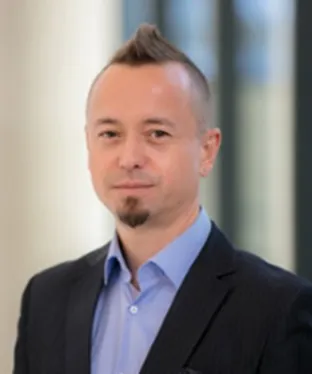
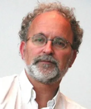
4. Prof. Fred Roozeboom, University of Twente, The Netherlands
K2-2: 11:30-12:15, Oct. 23, 2024, Wednesday
Title: Atomic Layer Processing: Its Evolution, Diverse Applications, and Future Prospects
Abstract:
In sub-10 nm scaling and fabrication of 3D architectures, especially the techniques of ALD and ALE have manifested to cost-effectively bridge the >10-years incubation time needed to bring EUV technology from prototype to commercial use. More importantly, these unique techniques can be used to create advanced devices by using dedicated isotropic (thermal and radical-enhanced) and anisotropic (directional and ion-enhanced) processing. Here, energetic species (radicals and/or ions in a plasma) are used in one or two steps, with the ions yielding anisotropic profiles (used in FinFET logic and 3D NAND memory), and neutrals and radicals yielding isotropic profiles used to deposit or etch the features in single-digit-nm device architectures containing horizontal nanowires, nanosheets and ‘forksheets’ in GAA-FETs, and complementary FETs.
Biography:
Prof. Dr. Fred Roozeboom received his MSc in chemistry (cum laude) from Utrecht University, Netherlands, in 1976, and his PhD in chemical engineering in 1980 at Twente University (Enschede, Netherlands) in heterogeneous catalysis.From 1980-1983 he worked on zeolite catalysis with Exxon/Mobil R&D Labs in Baton Rouge, USA (1980-1982) and with Exxon Chemicals in Rotterdam (1983).In 1983 he joined Philips Research (since 2006: NXP) in Eindhoven, Netherlands, where his early work encompassed MOCVD of III-V semiconductor lasers (1983-1988), IC metallization (1988-1990) and on bulk ferrite and thin-film soft-magnetic materials for magnetic recording (1990-1996). In 1996 he worked on MBE of ultrathin magnetic and ‘switchable mirror’ hydride multilayers.From 1997 to 2009 he led a team working on passive and heterogeneous integration, in particular on viahole technology and 3D integration for application in System-in-Package products and on high-value passives in silicon for application in wireless communication (RF decoupling), power management, and digital signal processing. Two technology transfers on 3D passive integration (PICS® wireless technology) to Philips' /NXP Semiconductor plants in Caen-France (now Murata Integrated Passive Solutions S.A.) and ASMC’s foundry in Shanghai-China resulted in over 400 M$ accumulated sales in the 2003-2008 period. For part of this work he received the Bronze Award of the ‘NXP Invention of the Year 2007’ and became an NXP Research Fellow in 2007. Another important application of the high-capacitance trench capacitor technology has been developed into miniaturized pacemaker production by Medtronic, USA, now used for minimum-invasive implantation.In 2009 he left NXP, and joined TNO-Holst Centre in Eindhoven, Netherlands, until 2021, as a senior technical advisor working in a team specializing in spatial Atomic Layer Deposition and related processing, e.g. Atomic Layer Etching and Cleaning (incl. EUV optics cleaning).In 2011, the spatial processing team at TNO received the 2nd EARTO Innovation Award.In 2014 he was elected Fellow of the Electrochemical Society.In 2023 he was elected as the recipient of the ECS Gordon E. Moore Medal, and also as Fellow of the American Vacuum Society, and winner of a 2023 Gerard & Anton High-Tech Star Award.
5. Prof. Boris Murmann, University of Hawaii, USA
K3-1: 9:00-9:45, Oct. 24, 2024, Thursday
Title: Integrated Circuit Innovation in the Age of AI
Abstract:
The field of machine learning and artificial intelligence has been a sleeping giant that was recently awakened by the enormous compute power of deeply scaled CMOS technology. The current sentiment suggests that AI capabilities will affect nearly all aspects of our lives, including the way we use and design the circuits that have enabled this movement in the first place. This talk will review the current trends in circuit design for AI/ML as well as opportunities in AI/ML for circuit design. As an overarching theme, I will highlight that circuit design must become more agile and open to attract new talents and to deliver future progress at the rate demanded by its driver applications.
Biography:
Dr. Boris Murmann is a Professor of Electrical & Computer Engineering at the University of Hawai'i at Manoa. From 2004-2023 he served as a Professor of Electrical Engineering at Stanford University. From 1994 to 1997, he was with Neutron Microelectronics, Hanau, Germany, where he developed low-power and smart-power ASICs. Since 2004, he has worked as a consultant with numerous Silicon Valley companies. Dr. Murmann’s research interests are in mixed-signal integrated circuit design, including sensor interfaces, A/D and D/A conversion, high-speed communication links, embedded machine learning (tinyML) as well as open-source chip design. He is a fellow of the IEEE and currently chairs the IEEE SSCS Technical Committee on the Open-Source Ecosystem.
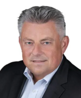
6. Prof. Albert Wang, University of California, Riverside, USA
K3-2: 9:45-10:30, Oct. 24, 2024, Thursday
Title: On-Chip ESD Protection: Methodologies, Challenges and Perspectives
Abstract:
No chip may be sold without ESD protection. On-chip ESD protection remains a major design challenge for ICs, especially for complex chips at advanced technology nodes, as well as for emerging heterogeneous integration (HI) technologies and integrated-systems-on-chiplets (SoIC). ESD protection design optimization, validation and prediction become very important to advanced ICs, which requires good ESD design methodologies. This paper reviews advances in on-chip ESD protection designs. Emerging ESD design challenges and future ESD protection perspectives will be highlighted.
Biography:
Prof. Albert Wang received the BS degree from Tsinghua University and the PhD degree from State University of New York at Buffalo. He is a Professor of Electrical and Computer Engineering at University of California, Riverside, USA. His research covers semiconductor devices, AMX/RF ICs, design-for-reliability for ICs, 3D heterogeneous integration, emerging devices and circuits, and LED visible light communications. He published two books and 320+ peer-reviewed papers, and holds 16 U.S. patents. His editorial board services include IEEE TCAS I, IEEE EDL, IEEE TCAS II, IEEE TED, IEEE JSSC, and IEEE TDMR. He is/was IEEE Distinguished Lecturer for IEEE EDS/CASS/SSCS. He was President of IEEE Electron Devices Society. His other committee services include the International Technology Roadmap for Semiconductor (ITRS), IEEE Heterogeneous Integration Roadmap (HIR), IEEE 5G Initiatives, IEEE Smart Lighting Project Roadmap and IEEE Fellow Committee. He was General Chair of IEEE EDTM2021 and IEEE RFIC2016. He was Program Director of National Science Foundation, USA. He was recipient IEEE J. J. Ebers Award and IEEE EDS Distinguished Service Award. Wang is a Fellow of National Academy of Inventors, an IEEE Fellow and an AAAS Fellow.
7. Prof. Youngcheol Chae, Yonsei University, Korea
K4-1: 9:00-9:45, Oct. 25, 2024, Friday
Title: CMOS Digital Radiography
Abstract:
Medical X-ray detectors such as computed tomography, radiography and dental X-ray are widely used in medical diagnostics. The market size of X-ray detector has also increased in recent years and the forecast is also very promising. The size of X-ray detectors must be the same size as the target, simply because the X-rays cannot be focused through a lens. The wafer-scale CMOS detector can be realized using the wafer-level stitching technique. Due to the volume-scale feasibility of the scintillator with CMOS pixels, CMOS X-ray detectors are not only cost-effective but also suitable for use in large detectors, thus dominating the X-ray imaging market. CMOS X-ray detectors used in medical devices should also provide full image depth for a given area of interest and require high resolution, low noise and wide dynamic range in a wafer-scale detector. Therefore, the CMOS X-ray detector poses significant challenges to the sensor and readout interfaces. It would be interesting to see how such challenges are adequately addressed in recent advances in wafer-scale CMOS X-ray detectors.
Biography:
Prof. Youngcheol Chae is currently a Professor in Electrical and Electronic Engineering at Yonsei University, Seoul, Korea. He received his Ph.D. degree from Yonsei University in 2009. During his Ph. D. studies, he advanced oversampling ADCs through innovative design techniques including inverter-based amplifiers, which have been adopted today for many low-power data converters. After joining Yonsei University in 2012, he led a Yonsei Mixed-Signal IC group, focusing on innovative analog and mixed-signal circuits and systems for communication, sensing, and biomedical applications. This has resulted in 130+ peer-reviewed journal and conference papers and holds 50+ patents. Especially, his research team reported 60+ State-of-The-Art Chips in JSSC, ISSCC, and Symposium on VLSI Circuits. Dr. Chae has been serving as a TPC member of the International Solid-State Circuits Conference (ISSCC), Asian Solid-State Circuits Conference (A-SSCC), and Custom Integrated Circuits Conference (CICC). He received the ISSCC 2021 Takuo Sugano Award for Outstanding Far-East Paper, the Best Young Professor Award in Engineering from Yonsei University in 2018, the Haedong Young Engineer Award from the Institute of Electronics and Information Engineers (IEIE) Korea in 2017, the ISSCC Silkroad Award in 2017, the Outstanding Research Award of Yonsei University (2017, 2019, and 2020), and the Outstanding Teaching Awards of Yonsei University (2013, 2014). He was a guest editor of the Journal of Solid-State Circuits (JSSC) and a distinguished lecturer (DL) of IEEE Solid-State Circuits Society (SSCS).
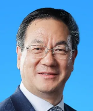
8. Prof. Chengjie Zuo, University of Science and Technology of China, China
K4-2: 9:45-10:30, Oct. 25, 2024, Friday
Title: High-Frequency and Wideband RF Filters for 6G and Wi-Fi 7
Abstract:
This talk will first give an overview on advanced chip-level RF filter technologies that have been developed and commercialized during the deployment of 3G, 4G and 5G wireless communications. These include the conventional SAW, BAW/FBAR, LTCC filters, as well as the emerging IHP-SAW, XBAR and Hybrid technologies. To further enhance filter performance for 6G and Wi-Fi 7 applications, three aspects of research have been pursued on next-generation acoustic resonators at the SRS lab of USTC. Lamb wave resonators at different Euler angles were studied on suspended X-cut LiNbO3 thin film to achieve quality factor (Q) larger than 100,000 at parallel resonance for a 6.5-GHz resonator. Fin-mounted design and half-electrode reflector were adopted to enable a 25-GHz A1-mode resonator that demonstrated the highest figure of merit (FoM of 21) among reported mmWave acoustic resonators in the 5G FR2 frequency range. Finally, a new kind of coupled shear mode SAW (X-SAW) resonator was proposed recently to break through the current limits on the conventional SAW technology, so as to achieve an extraordinarily large electromechanical coupling coefficient (k2) of 34% and high Bode-Qmax of 650 at 5 GHz, which has the potential to revolutionize the acoustic filter industry.
Biography:
Dr. Chengjie Zuo is a professor in the School of Microelectronics at the University of Science and Technology of China (USTC) and the founder of YUNTA Technologies. Dr. Zuo received the B.S. degree in electronic information science and technology from the University of Science and Technology of China (USTC), the M.Sc. degree (with honors) in electrical engineering from Delft University of Technology (TU Delft), and the Ph.D. degree in electrical and systems engineering from the University of Pennsylvania (Penn). Dr. Zuo is an IEEE senior member and a recipient of multiple awards including the IEEE Solid-State Circuits Society Predoctoral Fellowship. Dr. Zuo has published more than 50 papers, 140 US patent applications (among which 98 patents have been granted), and 120 Chinese patent applications.